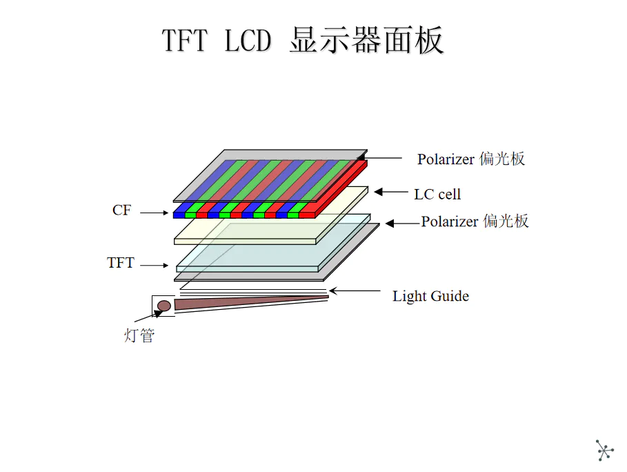
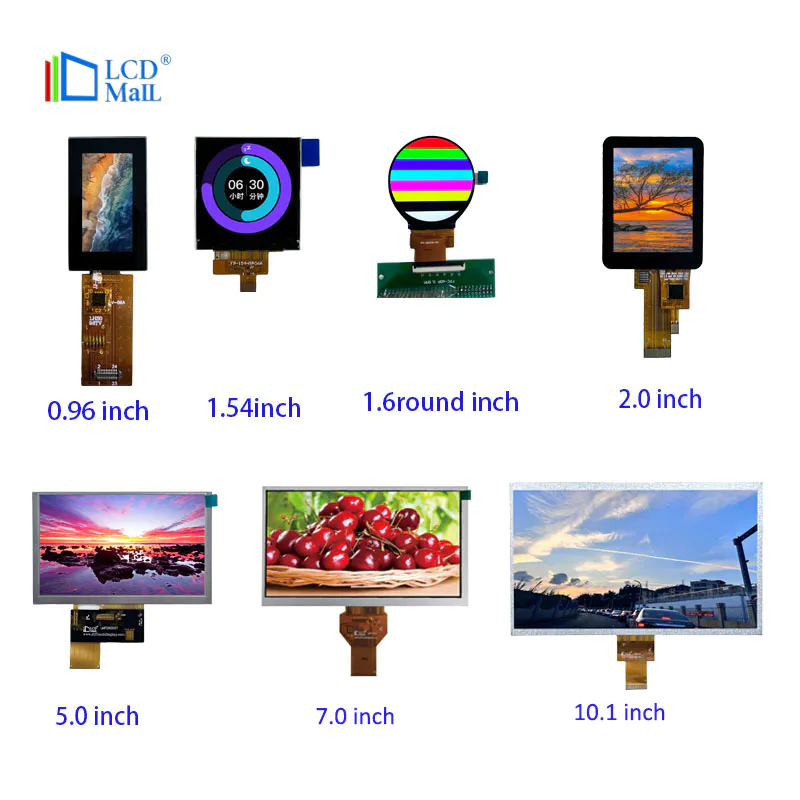
loading
LM-SPI-Module

high efficient oled displays prepared with the air-gapped bridges on quantum dot patterns for optical recycling

by:LCD Mall     2020-08-09
A structure with high optical efficiency is proposed and produced to realize the bright organic light emitting diode (OLED)
Display based on white OLED prepared with air-
Gap bridge on quantum dots (QD)patterns.
Compared with the traditional white OLED display, in our experiments, the optical strength of the proposed OLED display shows an enhancement of 58.
Red 2%, 16.
8% green after applying air-
Gap bridge structure on QD pattern with mass concentration of 20wt wt %.
This enhancement comes from the fact that the QD pattern converts unnecessary blue or blue/green light down to the required green or red light, as well as air-
Gap bridge improves the color conversion efficiency of QDs by using light recovery with full internal reflection (TIR)
In the interface.
In addition, the color range of the proposed OLED display is increased from 65. 5 to 75. 9% (NTSC x, y ratio)
Due to the narrow emission spectrum of QDs.
Non-polar ligand (oleic acid)-
The stamped Cadmium Selenium/zinc core/shell QDs were used.
First of all, the solvent exchange of red light QD is used for a rotary evaporator with a concentration of 50 mg PGMEA/ml (Heidolph, Hei-VAP)
, Also confirm that there is no aggregation of QDs.
Then, red QDs dissolved in PGMEA are mixed with positive PR (Merck, AZ GXR-601)
QDs with a concentration of 20wt wt %.
Because the main solvent of PR is PGMEA, the red QDs dissolved in PGMEA and PR are mixed well without other mixing processes.
Then, the exposure process of experimental optimization was carried out on the glass substrate; 1)
4000rpm rotating coating of 2 μm film thickness, 2)pre-
Bake at 90 °c, 3)exposure of i-
The line UV radiation energy is 825 mJ/cm using a mask alignment (
Microtec company, MA6), 4)
Immerse yourself in developers (
AZ 300 MIF)for 60u2009s, 5)
Hard baking at 110 ° c for 90 µs and 6)oxygen plasma (diener, ZEPTO)
Used to remove residual layers.
By repeating the above process, Green QDs were patterned on the same substrate, and red and green QD maps were realized.
Use a light mirror designed for air
A master Si, he has 5-μm-
The height pattern is made by a photo-taking process that subsequently reacts to ion etching.
Then, UV resin (
Minutes technology, minutes-ERM)
Assign on PET substrate and use Si master for imprint under pressure.
Air after full exposure to UV-
The gap bridge on the PET substrate is released from the Si master.
Custom message
Chat Online 编辑模式下无法使用
Leave Your Message inputting...
Thank you for your message! We are LCD Mall, committed to providing customers with high-quality services and products. Our salesperson will contact you as soon as possible. If you have urgent questions, please feel free to contact us directly through WhatsApp or email: WhatsApp: 86-13713689582/ info@AllTouchDisplay.com .